CONFERENCE DATES
7-10 July 2020
ABSTRACT SUBMISSION DEADLINE
15 June 2020
REGISTRATION OPTIONS
For the Live or Virtual Event
7-10 July 2020
15 June 2020
For the Live or Virtual Event
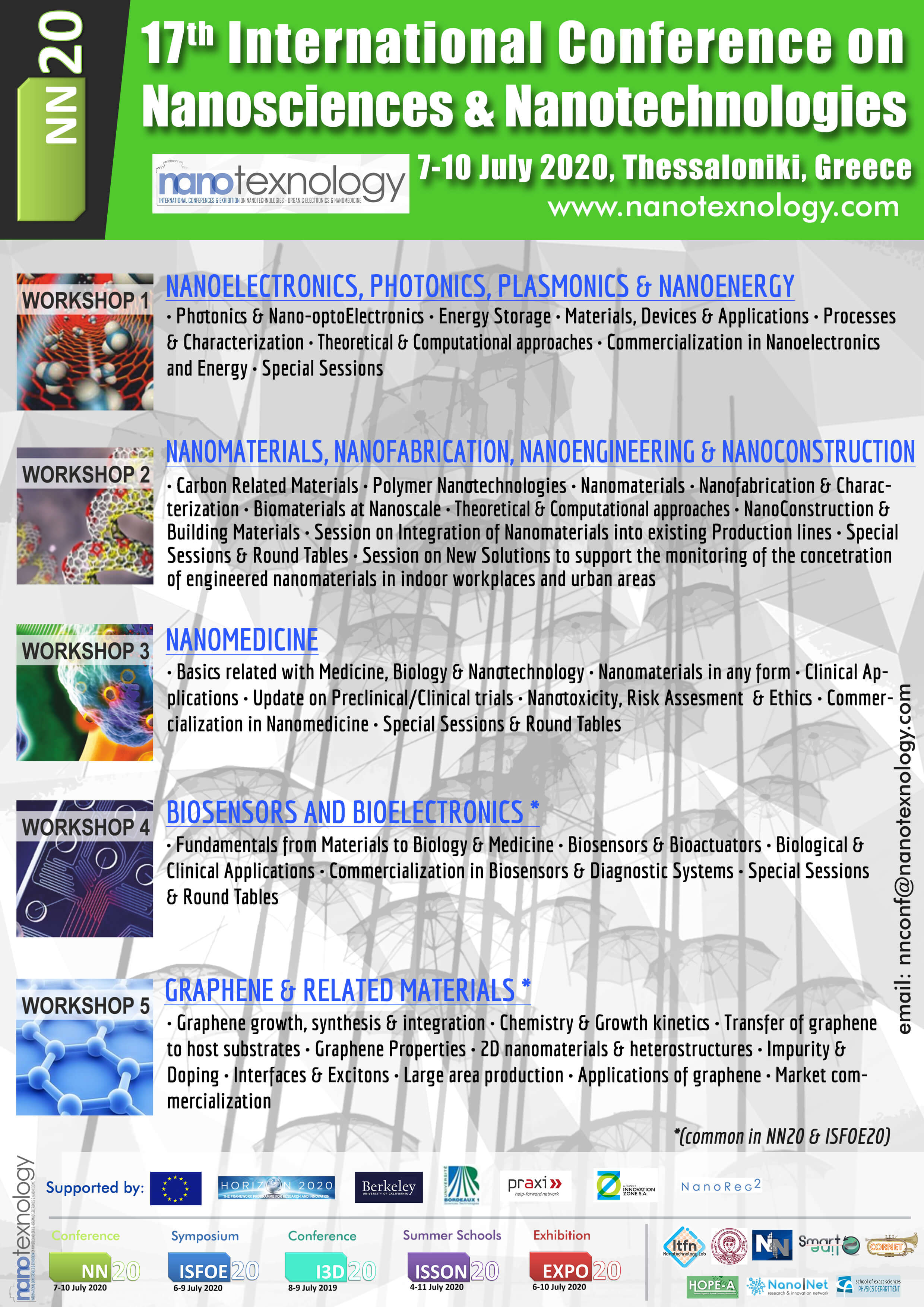
Nanoelectronics, Photonics, Plasmonics & Nanoenergy are among the most rapidly growing fields of modern science and technology. Nowadays, resources and investments by government agencies, research institutes and industries are devoted to the developments of materials, processes, instrumentation, equipment, devices, products and solutions for Nanoelectronics, Photonics & NanoEnergy.
The Workshop aims to foster research & collaborations and to serve as a forum for scientists, engineers, industrials professionals and policy makers from all the world where there will be exchange of information and access to the latest developments in photonics, nanoelectronics, materials, inorganic, organic and printed photovoltaics, device structures, system integrations, manufacturing processes, characterization and monitoring, product applications and business opportunities.
R. P. Silva (Chair), Nano-Electronics Centre, Advanced Technology Institute, Uni of Surrey, UK
S. Kassavetis (co-Chair), Nanotechnology Lab LTFN, AUTh, Greece
T. Anthopoulos, Physical Science & Engineering Div., KAUST, Saudi Arabia
V. Constantoudis, Inst. of Nanoscience and Nanotechnology, N.C.S.R. "Demokritos", Greece
M. Gioti, Nanotechnology Lab LTFN, AUTh, Greece
N. Kalfagiannis, School of Science & Technology, Nottingham Trent Uni., UK
J. - L. Lazzari, CNRS, Aix-Marseille University, CINaM, France
M. McLachlan, Dept. of Materials, Imperial College London, UK
K. Teshima, Center for Energy & Environmental Science, Shinshu University, Japan
![]()
![]()
![]()
![]()
![]()
![]()
![]()
![]()

![]()
![]()
![]()
![]()

![]()
![]()
![]()
![]()
![]()